
URL: https://www.desy.de/news/news_search/index_eng.html
Breadcrumb Navigation
DESY News: Scientists observe nanowires as they grow
News
News from the DESY research centre
Scientists observe nanowires as they grow
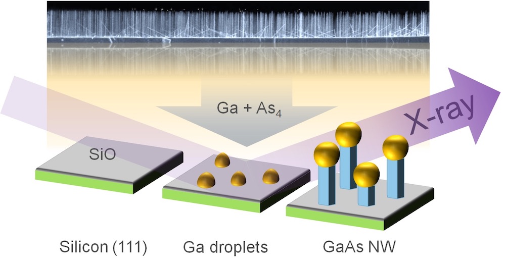
At DESY's X-ray source PETRA III, scientists have followed the growth of tiny wires of gallium arsenide live. Their observations reveal exact details of the growth process responsible for the evolving shape and crystal structure of the crystalline nanowires. The findings also provide new approaches to tailoring nanowires with desired properties for specific applications. The scientists, headed by Philipp Schroth of the University of Siegen and the Karlsruhe Institute of Technology (KIT), present their findings in the journal Nano Letters. The semiconductor gallium arsenide (GaAs) is widely used, for instance in infrared remote controls, the high-frequency components of mobile phones and for converting electrical signals into light for fibre optical transmission, as well as in solar panels for deployment in spacecraft.
To observe the growth as it takes place, Schroth's group installed a mobile experimental chamber, specially developed by KIT for X-ray experiments and partially funded by the Federal Ministry of Education and Research (BMBF), in the brilliant X-ray beam of DESY's synchrotron radiation source PETRA III at experimental station P09. At one-minute intervals the scientists took X-ray pictures, which allowed both the internal structure and the diameter of the growing nanowires to be simultaneously determined. In addition, they measured the fully-grown nanowires using the scanning electron microscope at the DESY NanoLab. “To ensure the success of such complex measurements, an extensive period of growth characterisation and optimisation at the UHV Analysis Lab at KIT was a prerequisite,” explains co-author Seyed Mohammad Mostafavi Kashani from University of Siegen.
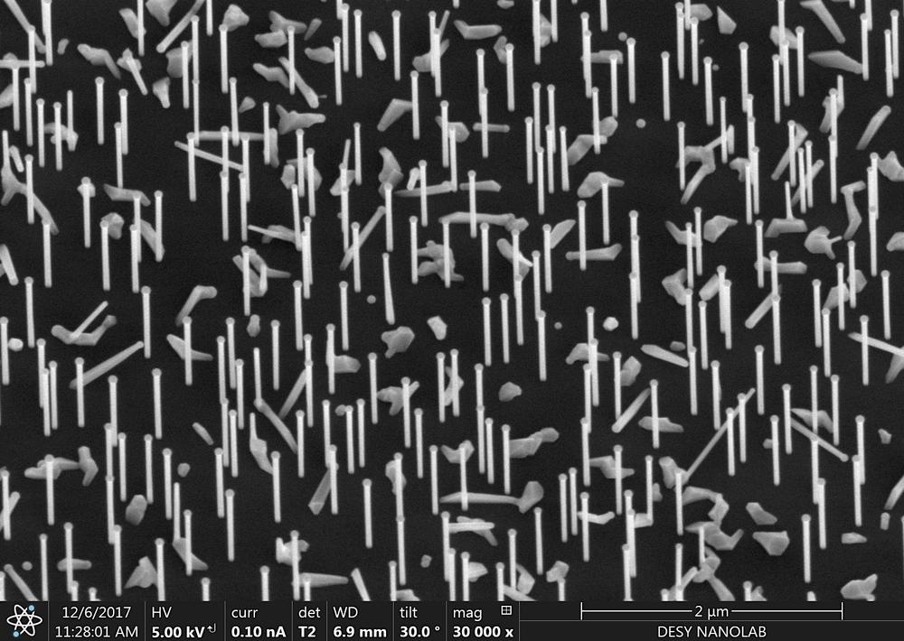
Nano forest: 'Aerial' view of the tiny wires growing on a silicon wafer, captured with a scanning electron microscope at the DESY NanoLab. Credit: DESY, Satishkumar Kulkarni/Thomas Keller
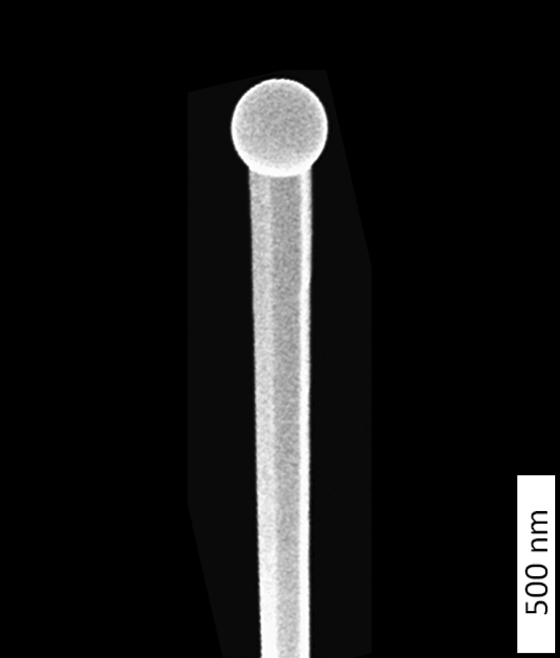
"One rather exciting feature is that the images taken under the electron microscope show the nanowires to have a slightly different shape," says co-author Thomas Keller from DESY NanoLab. Although the wires were thicker at the top than at the bottom, just as indicated by the X-ray data, the diameter measured under the electron microscope was larger in the lower region of the wire than what was observed using X-rays.
"We found out that the growth of the nanowires is not only due to the VLS mechanism but that a second component also contributes, which we were able to observe and quantify for the first time in this experiment. This additional sidewall growth lets the wires gain width," explains Schroth. Independently of VLS growth, the vapour deposited material also attaches itself directly to the side walls, particularly in the lower region of the nanowire. This additional contribution can be determined by comparing the X-ray measurements taken early on during the growth of the wire, with the electron microscope measurement after growth has ended.
Such detailed findings not only lead to a better understanding of the growth process; they also provide approaches for customising future nanowires to have special properties for specific applications - for example to improve the efficiency of a solar cell or a laser.
This research is also part of the strategic collaboration between the two Helmholtz Centres KIT and DESY, which are advancing this research within the Helmholtz programme "From Matter to Materials and Life" (MML).
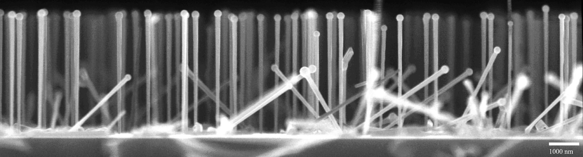
Electron microscope view of the fully grown nanowires.
Credit: KIT, Julian Jakob (Download [269 kB, 2048 x 553])
Reference:
“Radial Growth of Self-Catalyzed GaAs Nanowires and the Evolution of the Liquid Ga-Droplet Studied by Time-Resolved in situ X‐ray Diffraction”; Philipp Schroth, Julian Jakob, Ludwig Feigl, Seyed Mohammad Mostafavi Kashani, Jonas Vogel, Jörg Strempfer, Thomas F. Keller, Ullrich Pietsch, and Tilo Baumbach; Nano Letters, 2018; DOI: 10.1021/acs.nanolett.7b03486
