 MVD Telescope
DESY - Hall 2, Experimental Area 22
The ZEUS MVD Telescope is placed in the testbeam area 22 at
the DESY II testbeam.
If you would like to use the telescope during your testbeam
time, please contact
Ulrich Koetz
and Ingrid-Maria Gregor
well before the testbeam time.
Do not forget that you need to
request testbeam time before this.
We had to set up some rules for the use of the telescope to ensure that the telescope is continuously available for users:
- Do not remove any cables or modules from the telescope hardware in the testbeam area 22.
- Do not remove any cables from the trigger electronics inside the hut.
- Do not turn off the computers in the hut or remove any hardware from the computers.
In case you want to do one of the above, please discuss with us. We might have a different solution for your problem. Many thanks for your understanding.
Common problems while using the telescope:
Following we collect the most common errors which occur during testbeam time.Some sound rather stupid, but you have to consider that people tend to sleep not enough during test beam periods.
Reasons for no trigger:
- Beam shutter not open.
- Selection magnet not turned on.
- Trigger shifted out of beam axis.
- Trigger cables not connected to telescope DAQ.
- NIM crate power supply tripped (rare).
Reasons for problems with the sensors:
- Bias voltage turned off
- NIM crate power tripped
. Make sure that you switch to beam trigger in the control room before data taking (see below).
The Telescope:
The beam telescope depicted in testbeam are 22 was originally assembled by Uli Koetz for the beam tests of the ZEUS MVD. The beam telescope consists of three reference detector modules (Ref.det 1, 2 and 3). Each of them provides three space coordinates (x, y and z) for a track through the telescope. The modules are a version of a CERN development. They consist of two 300 mm thick single-sided silicon sensors of 32mm x 32mm size with a strip pitch of 25 um and a readout pitch of 50 mm; the strip directions of the two sensors in a module are perpendicular to each other. The 640 readout strips on each sensor are readout by the VA2 chips (VA2 chip product of IDE AS, Norway). All modules have a very good signal-to-noise (S/N) ratio for MIP, 80 < S=N < 130, (t least in theory) and a high intrinsic position resolution, 28 mm, as reported by Zeus. The device under test (DUT) and the telescope modules are mounted on a common optical bench. The DUT is mounted between the first and the second telescope modules and can be positioned via an xy table (not in place at the moment). All modules can be shifted in z along the optical bench. A coincidence of three of the four scintillator fingers located at both ends of the optical bench is used to generate a trigger. The whole telescope including trigger is located onto an optical bench. This bench is again mounted on a huge translation stage. The whole system is supposed to be aligned to the beam.
Sometimes the system is shifted by shifting the optical bench by accident or "playing" with the translation stage.
The center of the trigger fingers should be at 170cm height. With a plummet
you can check if the center is also in the right position. The beam axis
is painted (faintly) onto the floor.
Furthermore it is important to know that the optical bench and the translation
stage are galvanic separated (by highly sophisticated plastic pieces).
Technical Details:
Readout system (hardware in area):
In the recent years we tried to label all cables and all devices to help you to identify the hardware.
- Three silicon strip detectors on an optical bench.
- VME crate with:
- Sequencer V551B (physical address 0x880000) is 1-unit wide VME module that handles the Data Acquisition from multiplexing front-end chips. The module is well suited to handle the VA family of chips (produced by IDE AS, Oslo) but due to its flexibility it can also be used with similar chips (Amplex, Gasplex, etc.).
-
ADC V550A (physical address 0x860000):
channel 0 is used for telescope plane 1 (the one before the DUT),
channel 1 for telescope plane 2 (the one soon after the DUT) -
ADC V550C (physical address 0x90000):
channel 0 is not used
channel 1 is used for telescope plane 3.
- Trigger system: finger scintillators with small PMTs (and a trigger logic unit for the new EUDAQ based system)
- NIM crate with:
- power supply for photomultipliers (12V and 0-1V steering voltage)
- power supply for silicon strip detectors (0-60V)
- level shifter for analog signal from telescope
The VA2 chip:
As readout chip for the silicon sensors the Viking VA2 chip (IDE AScompany, Norway) was chosen. This chip has following main characteristics:
- 128 readout channels of analog signals from a detector, each of them includes charge sensitive pre-amplifier, CR-(RC)2 shaper and analog memory;
- integrated multiplexer used to dispatch all 128 analog signal to one output in a sequential readout mode;
- built-in test and control circuits, which include input multiplexer and shift-register to distribute test pulses through the chip channels;
- externally adjustable peaking time in a range from0.5 to 2 µs;
- noise performance 60? + 11?*pF for a peaking timeof 2 µs;
- dynamic range no less than 4 MIP for bipolar signals and 8 MIP for a single polarity;
- maximal readout rate up to 10 MHz;
- contact pads have a pitch of 50 µm, that meets demands of the most popular detector bonding;
The schematic of one readout channel of VA2 is shown below.
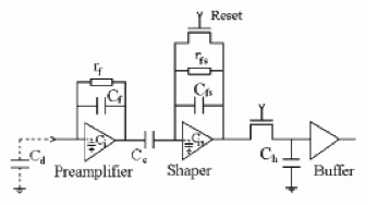
It integrates the charge sensitive preamplifier, the voltage controlled CR-(RC)2 shaper, the analog memory with the externally controlled track-n-hold circuitry. This readout system has a big flexibility, that allows to adjust allparameters when a maximum of speed or a minimum of noise is required in the experiment. 128 bit shift register controls the sequential readout process.
128 input pads are bonded to corresponding detector pads, from where the analog charge signal comes. After a physical event (a particle detection) each channel collects some charge. Then, after the peak of the pulse in the shaper has been reached, an external signal activates the analog memory of the chip, that fixes the peak voltage. Shifting a one bit through the control shift register multiplexes all analog channels outputs sequentially to one output of the chip, i.e. multiplexed readout is achieved. The output signal can be processed by a computer to obtain a spectrum. The chip can also work in a single channel mode. In this mode an arbitrary channel is selected through the control shift register, the analog memory circuits are disabled and it means the chip work as a simple pair of preamplifier-shapers. This mode is very useful for testing purposes and allows to estimate a pure noise performance of the readout system without an influence of high frequency digital circuits, which are used in a high speed sequential multiplexed readout.
The cabeling between the VME modules, the NIM modules and the patch panel in the test beam area is shown below:
.jpg)
The cabeling of the trigger logic in the test beam hut is shown here:
.jpg)
The details of how to use the DAQ of the telescope can be found here.
For details about the analysis of the data, please find more information here.
References:
- L. A. T. Bauerdick, Beam test of silicon strip sensors for the ZEUS
micro vertex detector, Nucl. Instr. and Meth. A 501 (2003) 340,
Available at: www.sciencedirect.com
- M. Milite, The internal structure of charmed jets in photoproduction at
HERA and tests of the ZEUS microvertex detector silicon sensors
Ph.D. Thesis, DESY-THESIS-2001-050, Available here
- M. Moritz, Measurement of the high Q2 neutral current DIS cross section at HERA, Ph.D. Thesis, DESY-THESIS-2002-009, Available here
- J. Velthuis, Results of 60Co irradiation of the ZEUS-MVD frontend chips, the Helix3.0, Ph.D. Thesis
- C. Colledani et al., Nucl. Instr. and Meth. A 372 (1996) 379
- J. Straver et al., Nucl. Instr. and Meth. A 348 (1994) 485.
Page maintained by: Ingrid-Maria Gregor last updated: 04.August 2010 Impressum (german); (English Translation)